GSS Benchmark
|
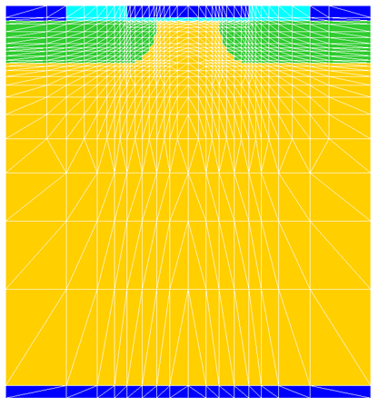
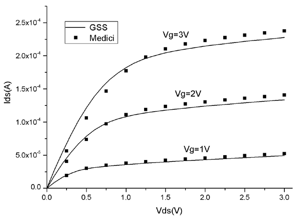
Several benchmark problems are solved by GSS for validating the arithmetic implementation. Here shows the 1µm, 0.35µm and 90nm channel length NMOS transistor benchmark test. The 1µm NMOS is taken from Medici's 1um MOS Template example. The device model is built by Medici and then converted to CGNS file with TIFTOOL. The mesh is shown as Fig(1). The source-drain IV characteristics are calculated both by GSS and Medici, keeping all the models and parameters unchanged. The results are listed in Fig(2). It shows both GSS and Medici give similar results. The little difference may be caused by the different implementation of transverse field dependent mobility.
Fig(1) The 1µm NMOS structure and mesh
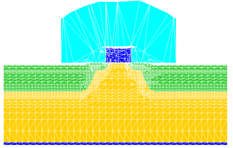
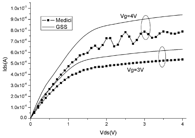
Fig(2) The source-drain IV curve The 0.35µm NMOS comes from Berkeley Baseline Report of "0.35µm CMOS PROCESS ON SIX-INCH WAFERS". This report provided TSUPREM4 input deck for process simulation and Medici input deck for device simulation. The device model used by GSS is got from TSUPREM4 simulation result by TIFTOOL and shown on Fig(3). I should say, the device model imported from process simulation has a very bad mesh quality and is not suitable for device simulation. Medici will stop working if Newton method is employed (However, Gummel method works.) and GSS also suffers from convergence problem. The final result shows on Fig(4). It seems that GSS calculates higher source-drain current than Medici do and Medici gives unphysical oscillation result when Vgs=4V.
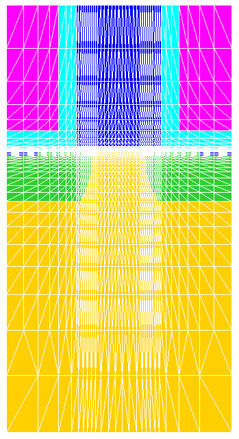
Fig(3) The 0.35µm NMOS structure and mesh
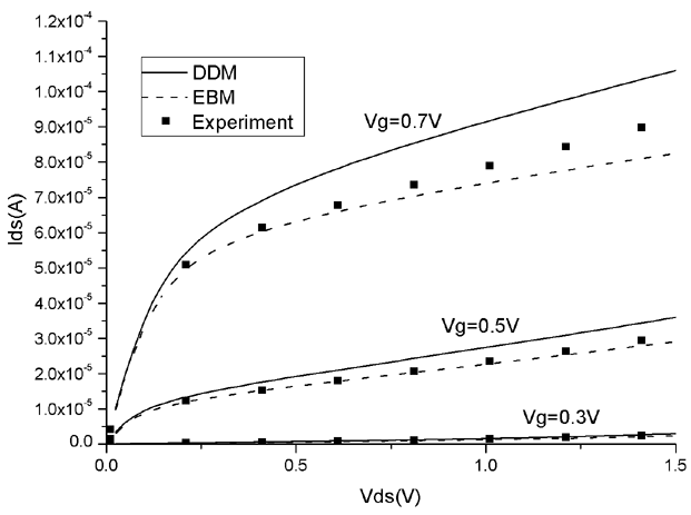
Fig(4) The source-drain IV curve of 0.35µm NMOS ˇˇ The 90nm NMOS is taken from "Well-Tempered" Bulk-Si NMOSFET Device Home Page, which offers well- characterized nanometer MOSFET for comparing existing simulation tools against real data. The device used by GSS is built as the suggestion of "Well-Tempered" project and shown as Fig(5). The simulation result achieved by DDM and EBM as well as experiment data are listed on Fig(6). The numerical result matches well with experiment data, especially the result calculated by energy balance method.
Fig(5) The 90nm NMOS structure and mesh
Fig(6) The source-drain IV curve of 90nm NMOS GSS: open source TCAD software. |
![]()